LALU:
Lookup
Arithmetic Logic Unit
MTM
Scientific, Inc
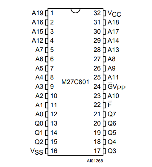
Figure 1: 8 MB EPROM with 20 Address Lines for use as LALU
This page describes the design and development of LALU: Lookup
Arithmetic Logic Unit. The LALU functions as the ALU for a simple
digital computer design in development. Traditionally an ALU is
included in the Central Processing Unit (CPU) of a computer. Stand
alone ALUs are also available, such as the venerable 74LS181. This page
describes using an 8 MB EPROM (M27C801: Organized as 1MB x 8 Bits) to
perform ALU functions on two 8-bit input registers "A" and "B".
The 8-bit output appears on IC pins Q7-Q0, which can then be
registered
back
into A.
Here are the assignments for the Accumulator "A", Register
"B" and
ALU Output (Registered into "A" by way of "C"). See diagram below.
B Register Inputs: A7, A6, A5, A4, A3, A2, A1, A0 (LSB)
A Register Inputs: A15, A14, A13, A12, A11, A10, A9, A8 (LSB)
ALU Output: Q7, Q6, Q5, Q4, Q3, Q2, Q1, Q0 (LSB)
LALU Function Select Inputs: A19, A18, A17, A16 (LSB)
The function to be performed by the LALU is chosen by using a 4
bit wide control nibble. A surprising variety of functions can be
performed with this simple architecture. Here is our assignment
for the 16 functions for LALU.
Control Name
Description (Result always sent to
A)
0000 AND
Logical AND of A and B
0001
OR
Logical OR of A and B
0010
NOT Logical NOT of A
0011
INC Increment A
by 1
0100
DEC Decrement A
by 1
0101
RLS Right
Logical Shift
0110
ADD Addition
(A+B)
0111
SUB Subtraction
(A-B)
1000
A>B Set Flag
IF A>B
1001
A=B Set Flag IF
A=B
1010
A<B Set Flag
IF A<B
1011
MBA Move B to A
1100
MUL Multiply
(A*B)
1101 A=0
Set Flag IF A=0
1110
OVF Set Flag IF
A+B>255
1111
LLS Left
Logical Shift
The LALU output is sent to holding Register C, and from there
forwarded to
"A" (during an ALU instruction). The flag functions of LALU
set a binary True/False output (1
or 0) in the LSB which is available for controlling conditional
jumps, or the flag can
be registered into "A". The flag for addition overflow is especially
useful for 16 bit addition. The Flags can be used for 4 different
conditional branches: A>B, A=B, A<B, A=0 and A+B>255. The A=0
flag is also very useful because the state does not depend on the
contents of Register B.
The list of functions chosen here for the LALU is basic.
LALU functions could include trigonometric quantities (sine,
cosine, etc), coefficients for calculations (FFT, infinite series,
etc), other logical functions (NAND, XOR, etc) as well as other flags,
bit shifts, rotates and support for complement
math. (Presently we use unsigned integer math.)
Here is a link to an early version of the HEX file we have defined
above. This file is
suitable for burning into an EPROM such as the M27C801: LALU.HEX
The HEX file for burning the EPROM is created using an Excel
spreadsheet
and hex file editor. We call this software the "Composer". The Excel
spreedsheet has 1,048,576 rows...
corresponding to the 1,048,576 memory locations in the EPROM.
Coincidentally, this was the largest number of rows possible in
a Microsoft Excel 2007 spreadsheet. The actual HEX file data appears in
column D. The
table is generated by using conditional logic formulas in the
cells of
column C. The A and B columns are inputs to the calculation.
(Representing registers
A and B) The large size of the spreadsheet file makes it
difficult to navigate. Hyperlink shortcuts were added to facilitate
navigation (See the hot links on the far righthand side of the
worksheet).
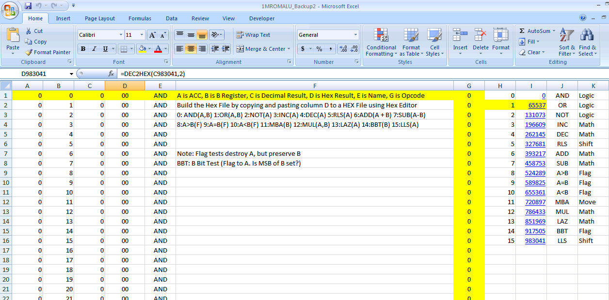
Figure 2: Excel Hex File composer for the LALU
A shortcoming of this LALU implementation is the
8-bit nature of register inputs A and B, as well as the output
result. A desirable feature for the LALU would be operation as a
bit-slice component. For example, in the case of
addition this would require routing an overflow signal to the next LALU
bit slice. Unfortunately, this would require dedicating a control line
address for the purpose. Consequently, the 4 address lines would be
reduced to 3, and instead of 16 functions the LALU would have
8. Larger programmable ROM's are available, although they present
challenges in terms of cost, programming hardware and hex file
creation.
Another real world shortcoming of the LALU is the speed of calcuation.
The M27C801
chosen here has an access time of 45ns. Many EPROMs have slower access
times. Another shortcoming is that a single-cell entry
mistake in the 1 million plus Excel spreadsheet would be
difficult to detect in practice.
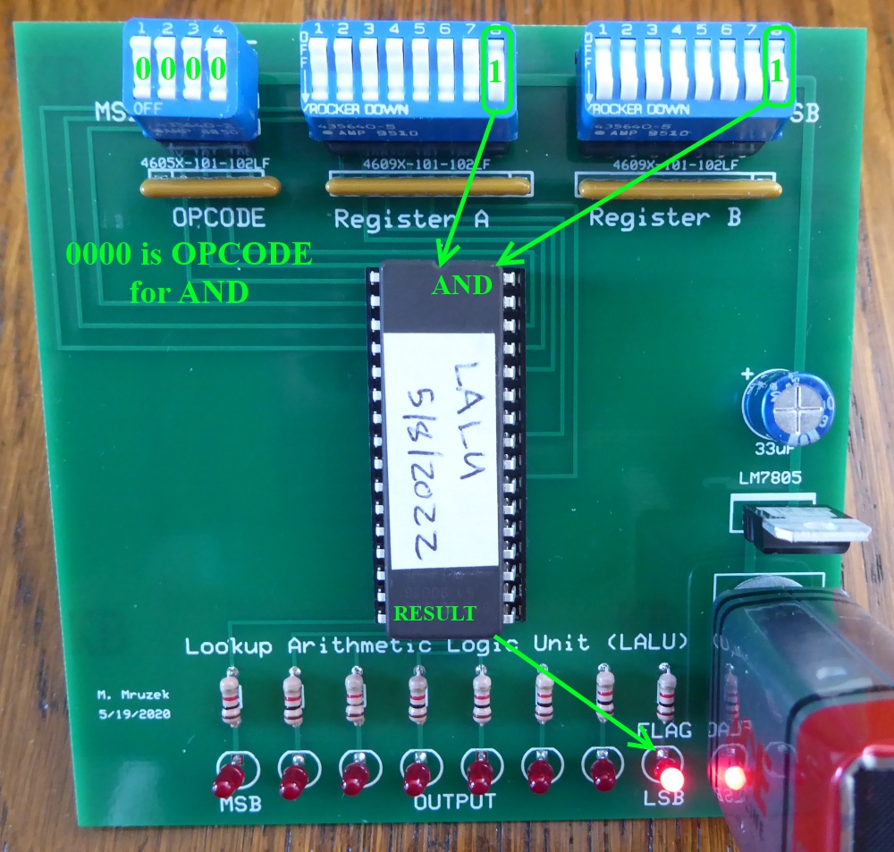
A PCB was designed to demonstrate the operation of LALU. The 4 bit
OPCODE and 8 bit registers "A" and "B" are set using DIP switches. In
the photo example the 4 bit OPCODE is set to "0000" which is the
logical AND operation. Examining the registers, we see the LSB of
both "A" and "B" are set high. Consequently, the AND operation result
sets the LSB of the result high, as indicated by the LED. We have found
this simple demonstration board very useful when writing code and are
unable to remember the specific behavior of an ALU function.
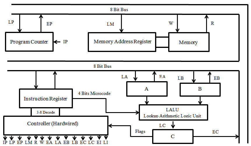
An 8-Bit computer to use the LALU Lookup Arithmetic Logic Unit was
designed and constructed. Here is a diagram of the LALU Computer
Architecture. This computer design has many similarities to the TTL-Retro Computer
we designed previously. The data and instruction bus width is 8 bits.
The shared memory holds both data and instructions. The single
byte is structured as follows: The top nibble is the instruction, and
the bottom nibble is 4 bits of microcode. Most of
the hardware control signals are for loading or enabling registers
with
respect to the bus. The controller for this version was hard-wired
using 'AND' and 'OR' 74LS series IC's.
The memory
is a combination of ROM and SRAM. Program code is placed in the ROM.
Note that LALU is capable of generating flags, which can be used
to perform conditional jumps.
With 4 bits in the top nibble, the LALU computer can have 16
instructions using a 4-16 decode. Our prototype LALU computer starts
with 8 instructions using a 3-8 decode. The instructions are:
0: NOP: No Operation
1: LDA: Load A from Memory
2: STA: Store A to Memory
3: MAB: Move Register A to Register B
4: ALU: Perform ALU operation (16 Microcoded Instructions)
5: JMP: Jump (Unconditional)
6: JIF: Jump (Conditional on Flag)
7: DTA: Direct to A (Immediate Load)
In the case of reading or writing to Memory (LDA and STA), the next
byte of the ROM program contains the address. In the case of a direct
load of A (DTA), the next byte of the ROM contains the data to load. In
the case of Jumps (JMP and JIF), the next byte of the ROM contains the
destination address (which must point to code!).
Here is a listing of the hardware signals generated by the Controller:
IP: Increment Program Counter
LP: Load Increment Counter (Jumps)
EP: Enable Program Counter on Bus
LM: Load Memory Address Register
R: Put Memory Contents on Bus (Pointer to memory is the Address
Register)
W: Put Bus Contents into Memory (Pointer to memory is the Address
Register)
EA: Enable A Register on the Bus
LA: Load A Register from the Bus
EB: Enable B Register on the Bus
LB: Load B Register from the Bus
EC: Enable C Register on the Bus
LC: Load C Register from LALU
LI: Load Instruction Register from the Bus
EI: Enable Instruction Register on the Bus
Not shown in the LALU Computer architecture drawing are a system clock
and a ring counter. The system clock allows optional choices for the
clocking: A manual ON-OFF toggle switch, a 555 timer running
at ~30HZ and a 1 MHZ crystal oscillator. The ring counter
generates 6 timing ticks from the system clock, for selective logical
operation of hardware by the controller. Any desired instruction can be
created using a glue-logic combination of ring counter ticks, system
clock ticks, and decoded instruction signals. Four bits of microcode
(lower nibble) are available to control the configuration of system
hardware, such as the LALU.
The most difficult part of the PCB design of the LALU computer has been
the hard-wired controller. Our long range plan is to replace the
hard-wired controller with a Lookup Controller. (See below!)
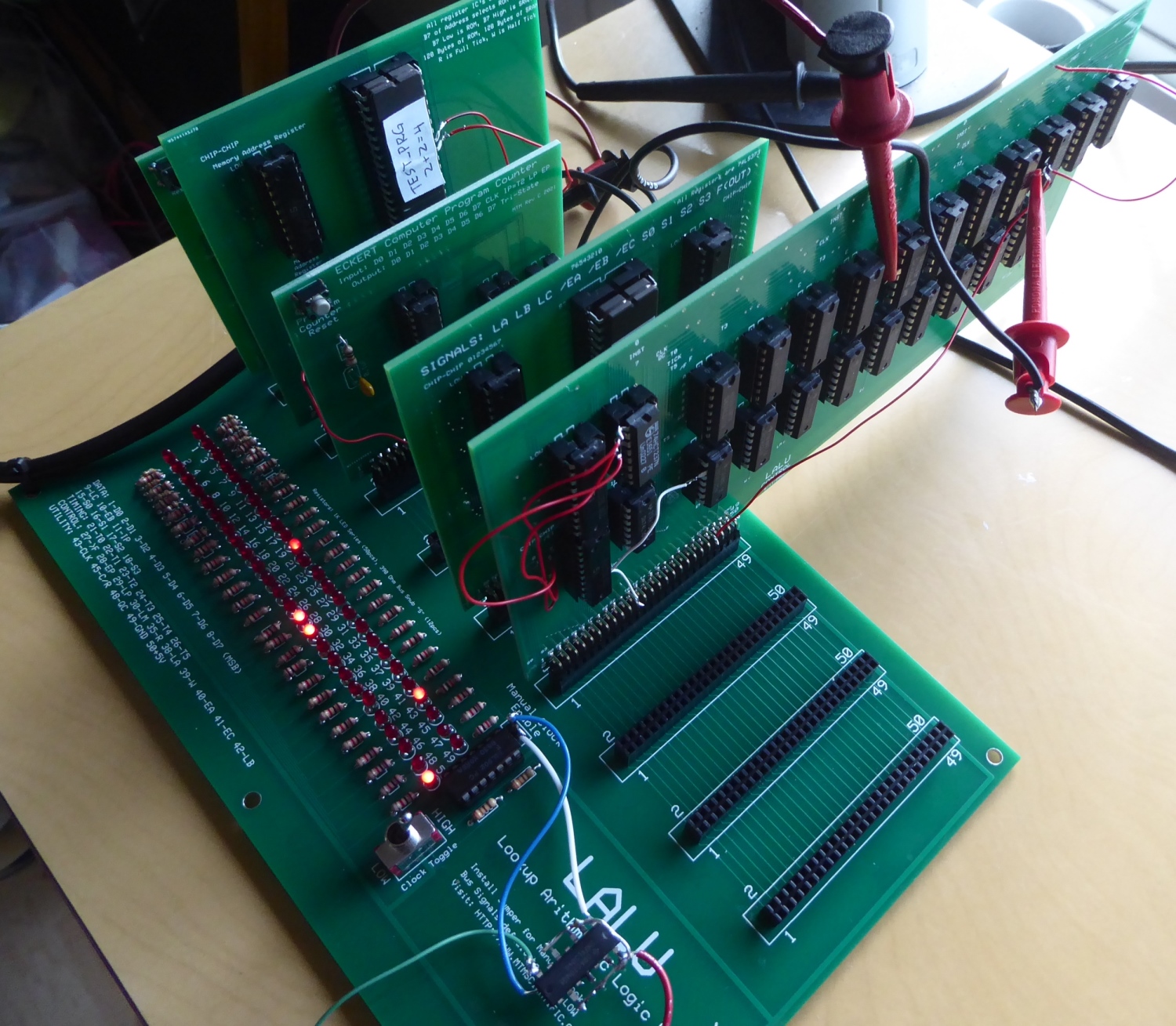
The PCB boards for this project were designed, purchased and assembled.
The 1st prototype had multiple wiring and logic errors. These were
subsequently fixed using point-to-point wiring. We eventually were able
to get the LALU Computer functional. This version of LALU has sinced
been updated to a Revision 2. Here is a photo of the LALU Computer
Prototype working on the test
bench:
PROJECT UPDATE (July 31, 2022):
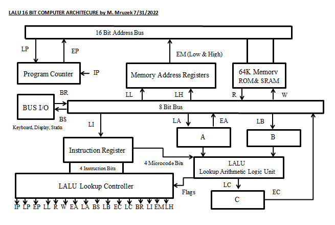
We have updated the LALU computer to use a 16 bit address bus, while
retaining the original 8 bit data bus. Here is an architecture layout
of the 16 bit version of LALU. With a 16 bit address bus the LALU
computer is capable of direct read and write to 64K of memory. We
have also added hardware control signals for doing bus input and
output. Bus control is used for devices such as a keyboard, LCD display
and hardware stacks. This design has been built and operated as a
prototype. This design uses both a Lookup Controller as well as a
Lookup ALU.
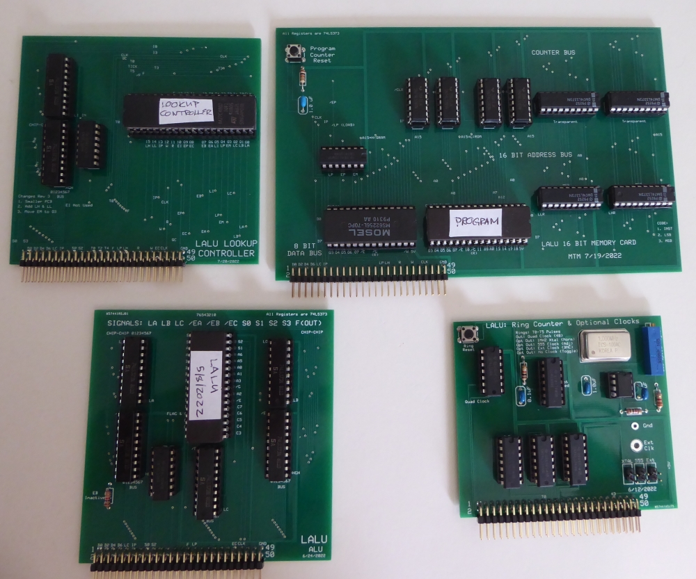
Here is a view of the Printed Circuit Boards comprising the 16 bit LALU
computer. The Lookup Controller card is compact, with minimal parts
count. We found it challenging to create the custom ROM to do the
controller lookups... A problem we eventually solved by creating a very
large EXCEL spreadsheet for the purpose.
There is a additional information about the LALU Computer at the AnyCPU
Forum. Here is a link to the LALU PROJECT
at AnyCPU.
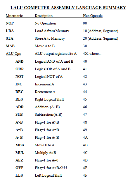
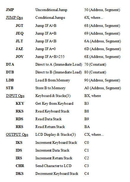
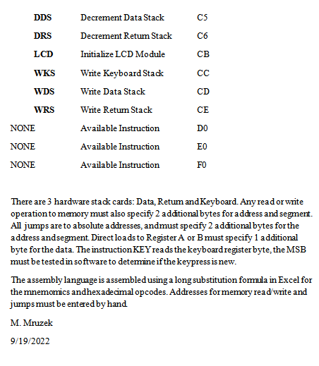
The Assembly Language for LALU is relatively simple. Here is
a listing of the instructions:
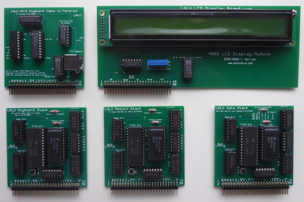
The LALU computer has 3 hardware stacks. They are the Data Stack,
Return Stack and Keyboard Stack. The LALU computer uses an LCD Display
Module to display text to the user. Input to the LALU computer is
provided by a standard PS/2 keyboard routed through a PIC
Microcontroller which provides 8-bit parallel bus output. This keyboard
and card combination was created to emulate an APPLE IIE keyboard. (As
used on our TTL-Retro Project.) Here is a photo of these various
cards.
We are presently in the process of writing a higher level language for
LALU using the Assembly Language as the first layer of code. The new
language is called "LANG", and it is an interpretive language with a
simple parser. LANG has some similarities to both Forth and Basic. LANG
is a stack based language. In the early days of computing it was not
uncommon to write your own homebrew languages for a personal computer.
Here is a link to an article in Kilobaud
Microcomputing Magazine about writing your own Forth Interpreter.
(Skip to page 76 in the magazine.) Here is the language specification
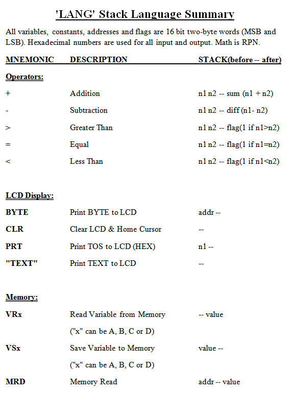
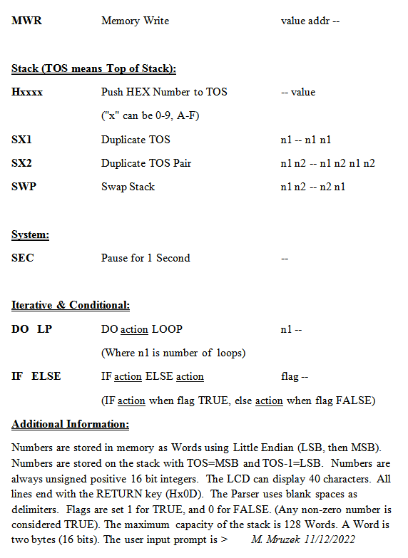
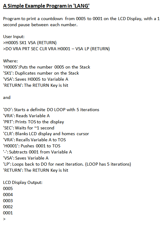
for LANG:
Here is a link to a Zip file containing the PCB Gerber files
for LALU Computer as of December, 2022: LALU
Gerbers
Here is a link to a Zip file containing the software and ROM code files
as of December, 2022: Code Files
Here is a link at the Vintage Computer Forum about some of the software
coding associated with LALU, and a discussion of predication. Vintage
Computer Forum.
UPDATE: LALU SBC (Single Board Computer)
In
the Spring of 2024 the LALU computer design was transferred to SBC
configuration (Single Board Computer). To minimize problems the
existing multicard PCB designs were combined onto a single PCB plane.
The attached photo shows the general layout. Another attached photo
shows the PCB with components populated.


The
LALU SBC V1 computer was found to have some minor layout issues.
Consequently a LALU SBC V2 was ultimately created. The SBC version of
LALU is intended for headless operation, with serial input and output
at 4800 baud, N-8-1. The complete set of LALU assembly language opcodes
is available. It was by using the assembly language opcodes and
homebrew assembler (WWA) that an interpreted language was created
called LANG. The LANG language has characteristics of both Forth
and Basic and is surprisingly fast.
Here is a link to a zip file containing the latest files for the SBC version:
LALU SBC
There are some interesting webpages to be found on the topic of lookup
ROMs. Here is an article about using ROM's for combinational logic.
http://39k.ca/using-roms-as-combinational-logic/
Here is a fantastic article from Garth Wilson about using ROM's for
lookup
tables.
http://wilsonminesco.com/16bitMathTables/
Bitwise operations are not native to Excel 2007. Here is a description
of how to add them using Visual Basic. (These were needed for creating
the Lookup ALU file for burning to ROM.)
https://stackpointer.io/software/bitwise-operations-excel-not-and-or-xor/281/